
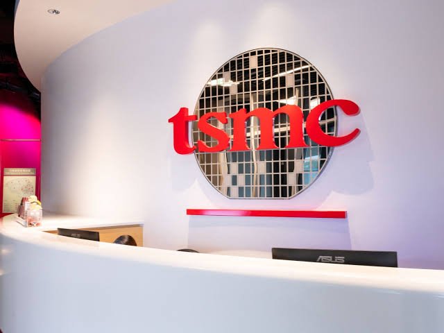

Taiwan has begun construction of a new semiconductor industrial park in the southern city of Kaohsiung, with TSMC set to anchor the project as demand for advanced packaging rises alongside artificial intelligence and high-performance computing.
The Baipu Industrial Park will serve as a testing and validation hub for equipment and materials used in advanced semiconductor packaging. TSMC, the world’s largest contract chipmaker, plans to establish two buildings at the site, including a technology-validation laboratory and a talent-training centre.
The TSMC facilities are expected to begin operations in the fourth quarter of 2029.
Proposal for Conducting Cyber Crisis Drill, Tabletop Exercise (TTEx) & CCMP Readiness Exercise
Advanced packaging becomes central to AI chip race
Advanced packaging is becoming increasingly important because the most powerful AI processors are no longer built as a single simple chip.
Instead, manufacturers increasingly combine multiple processors, memory components and specialised chiplets inside one tightly integrated package.
This allows companies to increase computing power without relying only on making individual transistors smaller.
TSMC’s packaging technologies are used in advanced AI chips designed by companies including Nvidia, AMD and Broadcom.
Taiwan President Lai Ching-te said at the groundbreaking ceremony that advanced packaging has become a critical part of global semiconductor competition as AI and high-performance computing expand.
The government expects the new park to allow equipment and material suppliers to test new technologies closer to TSMC before they enter mass production.
What advanced packaging actually means
Traditional semiconductor manufacturing focuses heavily on how small and powerful an individual chip can be made.
Advanced packaging focuses on what happens after those chips are produced.
Different computing components can be placed extremely close together and connected through high-speed links inside a single package.
That matters for AI because large models require processors and high-bandwidth memory to exchange enormous amounts of data very quickly.
TSMC’s CoWoS packaging technology has become particularly important in this market.
It is widely used to combine AI accelerators with high-bandwidth memory, allowing processors to access data much faster than through more conventional packaging designs.
Strong demand for AI accelerators has consequently turned packaging capacity into one of the semiconductor industry’s key bottlenecks.
Park will cover nearly 89 hectares
The Baipu Industrial Park will cover around 88.7 hectares, or roughly 219 acres.
About 53.6 hectares will be reserved for industrial use. TSMC will occupy the site with its two planned facilities, while the Kaohsiung city government will develop additional factory infrastructure for suppliers.
The park will complement TSMC’s existing advanced semiconductor operations at the nearby Nanzih Technology Industrial Park.
TSMC had already been working with Taiwan’s Ministry of Economic Affairs and Kaohsiung authorities on expanding testing and validation capability at Baipu. Earlier this month, a TSMC executive said closer collaboration with suppliers could improve validation efficiency by around 25% to 50%.
Taiwan wants equipment and material suppliers to perform more research and testing locally instead of relying on longer qualification processes elsewhere.
That could shorten the time between development of a new material or machine and its use inside a commercial semiconductor production line.
Taiwan expands packaging capacity beyond Kaohsiung
The Baipu project is part of a much larger expansion.
In July, Taiwan’s science and technology minister said TSMC would add two advanced packaging plants at the Chiayi Science Park in southern Taiwan. Chiayi is being developed into another major packaging hub.
The expansion reflects strong global demand for AI infrastructure.
TSMC has also begun building an advanced packaging facility at its Arizona semiconductor complex in the United States, while continuing to expand capacity in Taiwan.
Taiwan remains home to the world’s largest semiconductor manufacturing ecosystem, supported by major packaging, testing, equipment and material suppliers.
Companies including ASE Technology and Foxconn are also increasing investment in southern Taiwan.
Power supply remains critical to expansion
Large semiconductor facilities require enormous and highly reliable electricity supplies.
At the groundbreaking ceremony, Lai said Taiwan had assessed electricity requirements through 2035 and expected to maintain stable supply for industrial development.
Power availability has become an increasingly important issue as chipmakers expand fabrication, packaging and AI-related infrastructure simultaneously.
Taiwan’s challenge is therefore not only maintaining technological leadership but also providing enough energy, land and skilled workers to support continued growth.
The Baipu park addresses another major requirement: supplier proximity.
For advanced packaging, faster collaboration between TSMC and companies producing materials and equipment can shorten testing cycles and help new technologies reach volume production sooner.
That is particularly important as Nvidia, AMD, Broadcom and other chip designers compete to launch increasingly powerful AI processors.
What this means for you: Advanced packaging may sound like a specialised manufacturing issue, but it has become a major constraint on how quickly AI chips can be produced. Expanding packaging capacity could eventually improve supply of AI processors used in cloud services, data centres and high-performance computing.
Follow for daily updates on cybercrime, corporate fraud, DFIR, hacking, investigations, and digital forensics