
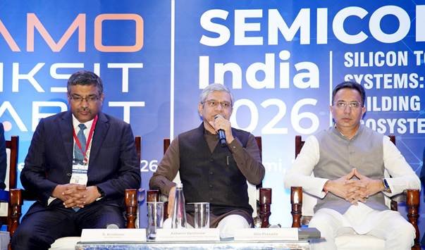

India’s semiconductor push has entered a new phase, with SEMICON India 2026 producing 11 major MoU exchanges and five announcements spanning chip manufacturing, packaging, equipment, materials, design and workforce development.
The Union Government said close to ₹1 lakh crore in investment commitments have already been received across the semiconductor ecosystem, with projects carrying the potential to create nearly 1 lakh employment opportunities.
The developments came as the government outlined its next-generation Semicon 2.0 strategy at the three-day industry event held at Yashobhoomi in New Delhi from September 17 to 19.
Unlike the first phase, which focused heavily on attracting large manufacturing projects, Semicon 2.0 is designed to build the wider ecosystem required around them — from chip design and fabrication equipment to advanced packaging, research and skilled technicians.
Proposal for Conducting Cyber Crisis Drill, Tabletop Exercise (TTEx) & CCMP Readiness Exercise
Tata, Nexperia and suppliers deepen manufacturing links
Among the agreements announced during the event, Tata Electronics signed an MoU with Netherlands-based Nexperia covering semiconductor wafer manufacturing, assembly and testing, technology collaboration and innovation.
Tata Electronics also entered an agreement with Ascendas Firstspace for development of a 363-acre vendor park in Dholera, Gujarat. The park is intended to bring suppliers closer to Tata’s planned semiconductor fabrication facility and build a supporting manufacturing cluster around it.
Suchi Semicon and eInfochips also marked the exchange of their first batch of commercial semiconductor devices.
The agreements illustrate an important change in India’s semiconductor strategy. Building a fabrication plant alone is not enough. Chip manufacturing depends on chemicals, gases, specialised machinery, packaging facilities, testing companies and hundreds of component suppliers operating around the main fab.
The government increasingly wants more of that value chain located within India.
SEMICON India 2026 drew more than 600 companies, with international firms accounting for roughly half of the exhibitors. The government said three of the 12 semiconductor projects approved under Semicon 1.0 have already entered commercial production.
What Semicon 2.0 changes
A semiconductor “fab” is the highly specialised factory where chips are physically manufactured on silicon wafers.
But the process does not end there.
Once chips are fabricated, they must be cut, packaged, tested and integrated into electronic products. Companies also need specialised materials, equipment, chip designs and trained engineers and technicians.
Semicon 2.0 is intended to strengthen these missing pieces.
Electronics and IT Minister Ashwini Vaishnaw said the programme will expand India’s semiconductor design ecosystem, strengthen precision manufacturing and train 1 lakh technicians required by new semiconductor facilities.
This is particularly important because semiconductor plants require highly specialised workers, and shortages in technical talent can become a bottleneck even when investment and factories are available.
India already has a major advantage in chip design. An EY-IESA report released around SEMICON India estimated that the country has roughly 20% of the world’s semiconductor design talent, while its semiconductor market could grow from about $64 billion in 2026 to $200 billion by 2035.
Global chipmakers are putting larger bets on India
The event also produced major investment announcements beyond the opening-day MoUs.
US semiconductor equipment giant Applied Materials announced plans to invest $5 billion in India over the next decade, focusing on research, supply-chain development and workforce expansion.
L&T Semiconductor Technologies separately unveiled 40 products, including its first silicon carbide chip aimed at electric vehicles and power systems.
The wider event eventually generated another wave of collaborations. On the second day alone, the government recorded 25 announcements and partnerships across manufacturing, materials, logistics, chip design, packaging, power electronics and workforce development.
The final session added another 15 announcements involving areas such as RISC-V processors, artificial intelligence, quantum platforms, fab automation and semiconductor training.
India is moving from incentives to actual production
India launched the original Semicon India Programme with an outlay of ₹76,000 crore to attract semiconductor and display manufacturing.
By February 2026, 10 projects involving expected investments of about ₹1.6 lakh crore had already received approval. The total later increased to 12 projects.
Yet India remains at an early stage compared with established semiconductor centres such as Taiwan, South Korea and the United States.
The next test is therefore execution.
Investment announcements must translate into operating factories, reliable suppliers and commercially competitive chips. Large fabrication projects also require enormous amounts of capital, power, water and specialised engineering expertise.
SEMICON India 2026 nevertheless shows that the policy focus is widening. India is no longer trying only to persuade global companies to build individual plants. It is attempting to develop the design, materials, machinery, packaging and workforce around those plants so that a larger part of the semiconductor supply chain stays within the country.
What this means for you: India’s semiconductor push could create opportunities well beyond chip engineers, including jobs in manufacturing, testing, electronics, equipment and supply chains. For students entering technical fields, the government’s plan to train 1 lakh semiconductor technicians signals where significant new demand may emerge.
Follow for daily updates on cybercrime, corporate fraud, DFIR, hacking, investigations, and digital forensics