
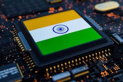
India has begun preparing for its next major leap in the semiconductor sector, with the government setting a target of developing advanced chip technology in the 7-nanometre to 3-nanometre range over the next eight years. Electronics and Information Technology Minister Ashwini Vaishnaw, while outlining the roadmap for Semicon 2.0, said India’s next phase of semiconductor development would go beyond chip fabrication and packaging. Chip design, manufacturing equipment, specialised materials, advanced packaging, research and talent development will also form part of the strategy.
India currently has 40-nanometre semiconductor technology. The government now plans to progressively move towards more advanced process nodes while simultaneously building the technical capabilities and skilled workforce required to support the transition. Over the coming years, the government plans to train one lakh semiconductor design engineers, with the broader objective of establishing India as a major global hub for chip design.
Algoritha Security Launches ‘Make in India’ Cyber Lab for Educational Institutions
What Will Semicon 2.0 Focus On Beyond Chip Manufacturing?
Chip design will be a key component of Semicon 2.0. The programme will focus on six major areas — computing, memory, radio frequency, power, networking and sensors. The government also plans to encourage domestic manufacturing of equipment used in semiconductor production. The objective is to reduce dependence on imports and build a wider industrial ecosystem capable of supporting semiconductor manufacturing within the country.
Semiconductor materials will also receive greater attention under the new programme. According to Vaishnaw, chip manufacturing can require between 150 and 500 specialised chemicals, gases and other materials. Developing domestic production capabilities for these inputs is therefore considered important for strengthening India’s semiconductor supply chain and reducing vulnerabilities arising from external dependence.
Under the first phase of the Semicon India Programme, 12 semiconductor units involving cumulative investments of around ₹1.77 lakh crore have been approved over the past five years. Three of these facilities have already entered commercial production. According to the minister, Micron began commercial production on February 28, 2026, followed by Kaynes on March 31 and CG Power on July 4. Construction is continuing at other approved facilities.
The government launched the Semicon India Programme in 2021 with an initial outlay of around ₹88,700 crore. The first phase primarily focused on establishing semiconductor fabrication and packaging facilities in India. Semicon 2.0 will now seek to develop the broader ecosystem by strengthening fabrication, chip design, materials, equipment, packaging and research capabilities together.
Global interest in India’s semiconductor sector has also increased. According to the government, international companies are investing more than ₹26,600 crore in India outside the Semicon India Programme. The government expects the country’s rapidly expanding electronics manufacturing industry to provide a strong domestic demand base for semiconductors.
How Is India Building a Skilled Semiconductor Workforce?
India has also been building its chip-design capabilities. Under the Chips to Startup Programme, Electronic Design Automation tools have been provided to more than 320 universities and startups. Using these resources, Indian students have developed 40 chip designs, which were presented to Prime Minister Narendra Modi during the previous Semicon India event.
The expansion of the skilled workforce is another major component of the strategy. The government had earlier set a target of creating a pool of 85,000 trained semiconductor engineers over 10 years. Under Semicon 2.0, that ambition is being raised to one lakh design engineers. Vaishnaw has also said that engineers working in India are already contributing to advanced chip designs at 2-nanometre and 3-nanometre process nodes for global semiconductor companies.
The government is also supporting semiconductor startups through the Design Linked Incentive scheme. A total of 105 startups have received support, with 24 receiving financial assistance of around ₹7,362 crore. Fifteen of these startups subsequently raised around ₹10,515 crore in venture capital funding, indicating growing investor interest in India’s semiconductor design ecosystem.
How Much Investment Has India Attracted in Semiconductors?
The semiconductor push is being supported by the rapid expansion of India’s electronics manufacturing industry. Electronics production in the country has crossed ₹11.5 lakh crore, while electronics exports have exceeded ₹4.26 lakh crore. More than 300 electronics manufacturing units are operating in the country, supporting around 25 lakh jobs. Mobile phones have also emerged as India’s largest export item.
However, reaching 3-nanometre technology will be a significant challenge. Leading global semiconductor companies have already advanced to 5-nanometre, 3-nanometre and 2-nanometre technologies. For India, the challenge is not limited to developing advanced chips. It also needs to build the equipment, materials, design capabilities, research infrastructure and skilled workforce required to sustain advanced semiconductor manufacturing.
Semicon 2.0 represents the next stage of that broader strategy. If India succeeds in moving from 7-nanometre towards 3-nanometre technology over the next eight years, it could strengthen the country’s position in the global semiconductor race and help it move beyond electronics manufacturing and chip packaging towards advanced chip design and manufacturing capabilities.
About the author — Ayesha Aayat writes on cybercrime, digital safety, and emerging online threats. Her work focuses on public awareness, legal clarity, and technology-driven risks.
Follow for daily updates on cybercrime, corporate fraud, DFIR, hacking, investigations, and digital forensics